- 您现在的位置:买卖IC网 > Sheet目录1918 > EFM32G230F128 (Energy Micro)IC MCU 32BIT 128KB FLASH 64QFN
...the world's most energy friendly microcontrollers
2013-06-28 - EFM32G230FXX - d0005_Rev1.60
51
www.energymicro.com
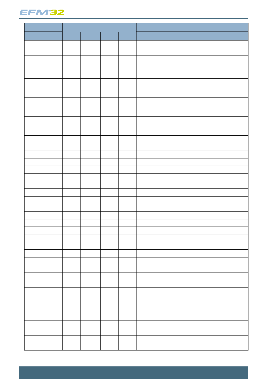
Alternate
LOCATION
Functionality
0
1
2
3
Description
HFXTAL_P
PB13
High Frequency Crystal positive pin.
I2C0_SCL
PA1
PD7
PC7
I2C0 Serial Clock Line input / output.
I2C0_SDA
PA0
PD6
PC6
I2C0 Serial Data input / output.
LETIM0_OUT0
PD6
PB11
PF0
PC4
Low Energy Timer LETIM0, output channel 0.
LETIM0_OUT1
PD7
PB12
PF1
PC5
Low Energy Timer LETIM0, output channel 1.
LEU0_RX
PD5
PB14
PE15
LEUART0 Receive input.
LEU0_TX
PD4
PB13
PE14
LEUART0 Transmit output. Also used as receive input in half duplex commu-
nication.
LEU1_RX
PC7
PA6
LEUART1 Receive input.
LEU1_TX
PC6
PA5
LEUART1 Transmit output. Also used as receive input in half duplex commu-
nication.
LFXTAL_N
PB8
Low Frequency Crystal (typically 32.768 kHz) negative pin. Also used as an
optional external clock input pin.
LFXTAL_P
PB7
Low Frequency Crystal (typically 32.768 kHz) positive pin.
PCNT0_S0IN
PC13
PC0
Pulse Counter PCNT0 input number 0.
PCNT0_S1IN
PC14
PC1
Pulse Counter PCNT0 input number 1.
PCNT1_S0IN
PC4
Pulse Counter PCNT1 input number 0.
PCNT1_S1IN
PC5
Pulse Counter PCNT1 input number 1.
PCNT2_S0IN
PD0
PE8
Pulse Counter PCNT2 input number 0.
PCNT2_S1IN
PD1
PE9
Pulse Counter PCNT2 input number 1.
TIM0_CC0
PA0
PD1
Timer 0 Capture Compare input / output channel 0.
TIM0_CC1
PA1
PD2
Timer 0 Capture Compare input / output channel 1.
TIM0_CC2
PA2
PD3
Timer 0 Capture Compare input / output channel 2.
TIM0_CDTI0
PA3
PC13
PF3
PC13
Timer 0 Complimentary Deat Time Insertion channel 0.
TIM0_CDTI1
PA4
PC14
PF4
PC14
Timer 0 Complimentary Deat Time Insertion channel 1.
TIM0_CDTI2
PA5
PC15
PF5
PC15
Timer 0 Complimentary Deat Time Insertion channel 2.
TIM1_CC0
PC13
PE10
Timer 1 Capture Compare input / output channel 0.
TIM1_CC1
PC14
PE11
Timer 1 Capture Compare input / output channel 1.
TIM1_CC2
PC15
PE12
Timer 1 Capture Compare input / output channel 2.
TIM2_CC0
PA8
PC8
Timer 2 Capture Compare input / output channel 0.
TIM2_CC1
PA9
PC9
Timer 2 Capture Compare input / output channel 1.
TIM2_CC2
PA10
PC10
Timer 2 Capture Compare input / output channel 2.
US0_CLK
PE12
PC9
USART0 clock input / output.
US0_CS
PE13
PC8
USART0 chip select input / output.
US0_RX
PE11
PC10
USART0 Asynchronous Receive.
USART0 Synchronous mode Master Input / Slave Output (MISO).
US0_TX
PE10
PC11
USART0 Asynchronous Transmit.Also used as receive input in half duplex
communication.
USART0 Synchronous mode Master Output / Slave Input (MOSI).
US1_CLK
PB7
PD2
USART1 clock input / output.
US1_CS
PB8
PD3
USART1 chip select input / output.
US1_RX
PC1
PD1
USART1 Asynchronous Receive.
USART1 Synchronous mode Master Input / Slave Output (MISO).
发布紧急采购,3分钟左右您将得到回复。
相关PDF资料
EFM32G232F64
IC MCU 32BIT 64KB FLASH LQFP64
EFM32G280F64
MCU 32BIT 64KB FLASH 100-LQFP
EFM32G290F64
MCU 32BIT 64KB FLASH 112-BGA
EFM32G840F64
MCU 32BIT 64KB FLASH 64-QFN
EFM32G842F64
IC MCU 32BIT 64KB FLASH LQFP64
EFM32G880F128
IC MCU 32BIT 128KB FLASH 100QFP
EFM32G890F64
MCU 32BIT 64KB FLASH 112-BGA
EFM32GG230F512
IC MCU 32BIT 512KB FLASH 64QFN
相关代理商/技术参数
EFM32G230F128G-E-QFN64R
功能描述:128K FLASH, 16K RAM, AES 制造商:silicon labs 系列:Gecko 包装:剪切带(CT) 零件状态:在售 核心处理器:ARM? Cortex?-M3 核心尺寸:32-位 速度:32MHz 连接性:I2C,IrDA,智能卡,SPI,UART/USART 外设:欠压检测/复位,DMA,POR,PWM,WDT I/O 数:56 程序存储容量:128KB(128K x 8) 程序存储器类型:闪存 EEPROM 容量:- RAM 容量:16K x 8 电压 - 电源(Vcc/Vdd):1.98 V ~ 3.8 V 数据转换器:A/D 8x12b,D/A 2x12b 振荡器类型:内部 工作温度:-40°C ~ 85°C(TA) 封装/外壳:64-VFQFN 裸露焊盘 供应商器件封装:64-QFN(9x9) 标准包装:1
EFM32G230F128-QFN64
制造商:Energy Micro AS 功能描述:MCU, 128K FLASH, USART+UART 3, QFN64 - Tape and Reel 制造商:Energy Micro AS 功能描述:MCU, 128K FLASH, USART+UART 3, QFN64 - Cut TR (SOS) 制造商:Energy Micro 功能描述:energy micro EFM32G230F128-QFN64 Microcontrollers (MCU) 制造商:Energy Micro AS 功能描述:IC MCU 32BIT 128KB FLASH 64QFN
EFM32G230F128-QFN64T
制造商:Energy Micro AS 功能描述:MCU, 128K FLASH, USART+UART 3, QFN64 - Trays
EFM32G230F128-QFN64-T
制造商:Energy Micro AS 功能描述:IC MCU 32BIT 128KB FLASH 64QFN
EFM32-G230F128-SK
功能描述:IC MICRO KIT GECKO 64QFN RoHS:是 类别:套件 >> 半导体产品 - IC 元件分类 系列:Gecko 其它有关文件:NXPLOGIC2-KIT-ND Contents 标准包装:1 系列:74AUP 套件类型:逻辑 值:180 件 - 18 种值各 10 件 包装:- 安装类型:表面贴装 包括封装:6-XSON,8-XSON,8-XQFN 产品目录页面:2653 (CN2011-ZH PDF) 工具箱内容:(10) 568-4391-1-ND - IC GATE MULT-FUNC CONFIG 6-XSON(10) 568-4390-1-ND - IC CONFIG MULT-FUNC GATE 6-XSON(10) 568-4389-1-ND - IC GATE DUAL FUNCTION 8-XSON(10) 568-4388-1-ND - IC GATE DUAL FUNCTION 8-XQFN(10) 568-4387-1-ND - IC F-F D-TYPE POS EDGE 8-XSON(10) 568-4386-1-ND - IC F-F D-TYPE POS EDGE 8-XQFN(10) 568-4385-1-ND - IC CONFIG MULTI-FUNC GATE 6-XSON(10) 568-4384-1-ND - IC EX-OR GATE 3-IN 6-XSON(10) 568-4383-1-ND - IC F-F D-TYPE POS EDGE 6-XSON(10) 568-4382-1-ND - IC LATCH D-TYPE 6-XSON更多... 其它名称:NXPLOGIC2-KIT
EFM32G230F128-T
制造商:Energy Micro AS 功能描述:IC MCU 32BIT 128KB FLASH 64QFN
EFM32G230F32
功能描述:ARM微控制器 - MCU 32KB FLASH 8KB RAM 32MHZ 1.8-3.8V
RoHS:否 制造商:STMicroelectronics 核心:ARM Cortex M4F 处理器系列:STM32F373xx 数据总线宽度:32 bit 最大时钟频率:72 MHz 程序存储器大小:256 KB 数据 RAM 大小:32 KB 片上 ADC:Yes 工作电源电压:1.65 V to 3.6 V, 2 V to 3.6 V, 2.2 V to 3.6 V 工作温度范围:- 40 C to + 85 C 封装 / 箱体:LQFP-48 安装风格:SMD/SMT
EFM32G230F32-QFN64
制造商:Energy Micro AS 功能描述:MCU, 32K FLASH, USART+UART 3, QFN64 - Tape and Reel 制造商:Energy Micro AS 功能描述:IC MCU 32BIT 32KB FLASH 64QFN